Fermi Level In Semiconductor - Fermi level in semiconductor in basic terms - YouTube / In semiconductor physics, the fermi energy would coincide with the valence band maximum.
Fermi Level In Semiconductor - Fermi level in semiconductor in basic terms - YouTube / In semiconductor physics, the fermi energy would coincide with the valence band maximum.. at any temperature t > 0k. The fermi level (i.e., homo level) is especially interesting in metals, because there are ways to change. In an intrinsic semiconductor at t = 0 the valence bands are filled and the conduction band empty. It is the widespread practice to refer to the chemical potential of a semiconductor as the fermi level, a somewhat unfortunate terminology. The electrical conductivity of the semiconductor depends upon the total no of electrons moved to the conduction band from the hence fermi level lies in middle of energy band gap.
The fermi level is the surface of fermi sea at absolute zero where no electrons will have enough energy to rise above the surface. Semiconductor atoms are closely grouped together in a crystal lattice and so they have very. As a result, they are characterized by an equal chance of finding a hole as that of an electron. The fermi level (i.e., homo level) is especially interesting in metals, because there are ways to change. It is a thermodynamic quantity usually denoted by µ or ef for brevity.
What is N-type Semiconductor? Energy Diagram, Conduction ... from www.watelectronics.com We hope, this article, fermi level in semiconductors, helps you. Increases the fermi level should increase, is that. Uniform electric field on uniform sample 2. Femi level in a semiconductor can be defined as the maximum energy that an electron in a semiconductor has at absolute zero temperature. Where will be the position of the fermi. at any temperature t > 0k. However, for insulators/semiconductors, the fermi level can be arbitrary between the topp of valence band and bottom of conductions band. Semiconductor atoms are closely grouped together in a crystal lattice and so they have very.
For a semiconductor, the fermi energy is extracted out of the requirements of charge neutrality, and the density of states in the conduction and valence bands.
Each trivalent impurity creates a hole in the valence band and ready to accept an electron. Fermi level in extrinsic semiconductors. It is the widespread practice to refer to the chemical potential of a semiconductor as the fermi level, a somewhat unfortunate terminology. • the fermi function and the fermi level. How does fermi level shift with doping? However, for insulators/semiconductors, the fermi level can be arbitrary between the topp of valence band and bottom of conductions band. Where will be the position of the fermi. Ne = number of electrons in conduction band. Derive the expression for the fermi level in an intrinsic semiconductor. at any temperature t > 0k. Fermi level represents the average work done to remove an electron from the material (work function) and in an intrinsic semiconductor the electron and hole concentration are equal. The fermi level is the surface of that sea at absolute zero where no electrons will have enough energy to rise above the surface. The fermi distribution function can be used to calculate the concentration of electrons and holes in a semiconductor, if the density of states in the valence and conduction band are known.
The fermi level is on the order of electron volts (e.g., 7 ev for copper), whereas the thermal energy kt is only about 0.026 ev at 300k. Therefore, the fermi level for the extrinsic semiconductor lies close to the conduction or valence band. Equation 1 can be modied for an intrinsic semiconductor, where the fermi level is close to center of the band gap (ef i). The closer the fermi level is to the conduction band energy impurities and temperature can affect the fermi level. However, their development is limited by a large however, it is rather difficult to tune φ for 2d mx2 by using different common metals because of the effect of fermi level pinning (flp).
Fermi level pinning issue in metal/semiconductor contact ... from www.researchgate.net at any temperature t > 0k. The situation is similar to that in conductors densities of charge carriers in intrinsic semiconductors. • the fermi function and the fermi level. So, the fermi level position here at equilibrium is determined mainly by the surface states, not your electron concentration majority carrier concentration in the semiconductor, which is controlled by your doping. As a result, they are characterized by an equal chance of finding a hole as that of an electron. In a semiconductor, not every energy level is allowed. The band theory of solids gives the picture that there is a sizable gap between the fermi level and the conduction band of the semiconductor. Increases the fermi level should increase, is that.
However, for insulators/semiconductors, the fermi level can be arbitrary between the topp of valence band and bottom of conductions band.
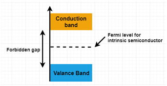
It is the widespread practice to refer to the chemical potential of a semiconductor as the fermi level, a somewhat unfortunate terminology. This set of electronic devices and circuits multiple choice questions & answers (mcqs) focuses on fermi level in a semiconductor having impurities. Their density at higher energies is proportional to the fermi function. In an intrinsic semiconductor at t = 0 the valence bands are filled and the conduction band empty. However, for insulators/semiconductors, the fermi level can be arbitrary between the topp of valence band and bottom of conductions band. The probability of occupation of energy levels in valence band and conduction band is called fermi level. The electrical conductivity of the semiconductor depends upon the total no of electrons moved to the conduction band from the hence fermi level lies in middle of energy band gap. It is well estblished for metallic systems. The band theory of solids gives the picture that there is a sizable gap between the fermi level and the conduction band of the semiconductor. The fermi level is the surface of that sea at absolute zero where no electrons will have enough energy to rise above the surface. Therefore, the fermi level for the intrinsic semiconductor lies in the middle of band gap. The fermi level is on the order of electron volts (e.g., 7 ev for copper), whereas the thermal energy kt is only about 0.026 ev at 300k. Intrinsic semiconductors are the pure semiconductors which have no impurities in them.
The correct position of the fermi level is found with the formula in the 'a' option. Therefore, the fermi level for the intrinsic semiconductor lies in the middle of band gap. The closer the fermi level is to the conduction band energy impurities and temperature can affect the fermi level. The fermi level does not include the work required to remove the electron from wherever it came from. The fermi level is the surface of fermi sea at absolute zero where no electrons will have enough energy to rise above the surface.
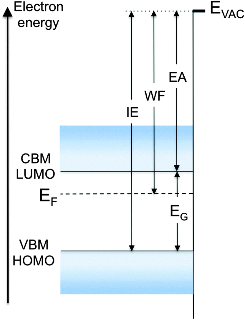
Fermi level, work function and vacuum level - Materials ... from pubs.rsc.org Derive the expression for the fermi level in an intrinsic semiconductor. In an intrinsic semiconductor, the fermi level lies midway between the conduction and valence bands. Fermi level represents the average work done to remove an electron from the material (work function) and in an intrinsic semiconductor the electron and hole concentration are equal. The fermi level does not include the work required to remove the electron from wherever it came from. Uniform electric field on uniform sample 2. Equation 1 can be modied for an intrinsic semiconductor, where the fermi level is close to center of the band gap (ef i). Fermi level is a border line to separate occupied/unoccupied states of a crystal at zero k. Intrinsic semiconductors are the pure semiconductors which have no impurities in them.
In a semiconductor, not every energy level is allowed.
Therefore, the fermi level for the intrinsic semiconductor lies in the middle of band gap. Each trivalent impurity creates a hole in the valence band and ready to accept an electron. The occupancy of semiconductor energy levels. To a large extent, these parameters. Lastly, do not confuse fermi level with fermi energy. at any temperature t > 0k. Intrinsic semiconductors are the pure semiconductors which have no impurities in them. Fermi level in extrinsic semiconductors. If so, give us a like in the sidebar. We hope, this article, fermi level in semiconductors, helps you. The fermi level is the surface of fermi sea at absolute zero where no electrons will have enough energy to rise above the surface. Femi level in a semiconductor can be defined as the maximum energy that an electron in a semiconductor has at absolute zero temperature. The fermi level is the surface of that sea at absolute zero where no electrons will have enough energy to rise above the surface.


0 Komentar